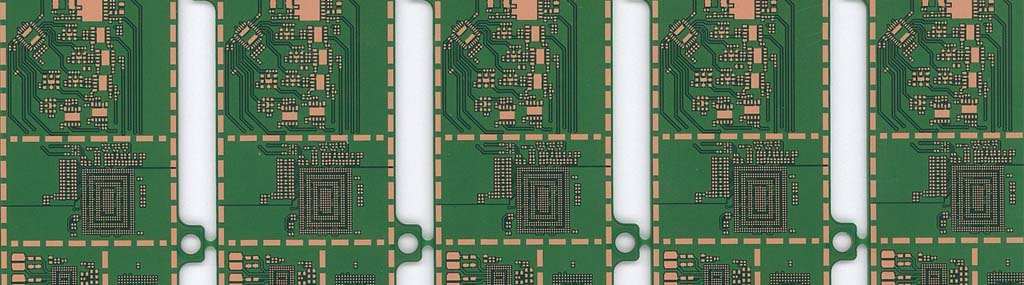
Due to the increased requirements to circuits by continuing miniaturization in final products, normal multilayer PCB can’t fulfil these requests. A special technology with finer track widths and smaller plated through holes is needed.
For this technical demand we offer the HDI-Technology. It is characterized by finest track widths (under 120 mic are feasible), smaller plated through holes (micro vias) and best heat dissipation by filled micro vias. Also a high quantity of layers is possible.
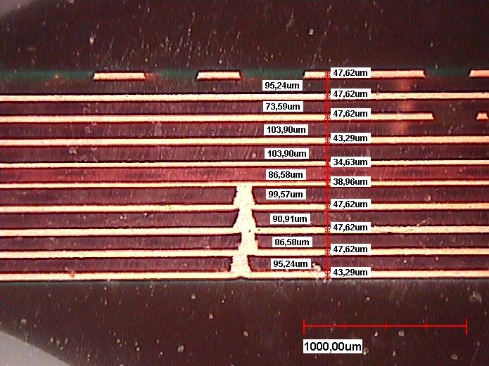
Micro section of a HDI-PCB
 For the production of HDI technology, we recommend you our audited and qualified partners in Asia. For further information, please contact us.
 English
 German