 As a further service, B&B provides high-grade micro section analysis and layer thickness tests. With the micro section analysis we measure the micro section samples individually to check the manufactured PCBs according to customer requests. For this quality service we are using micro section samples which were delivered or created in-house.
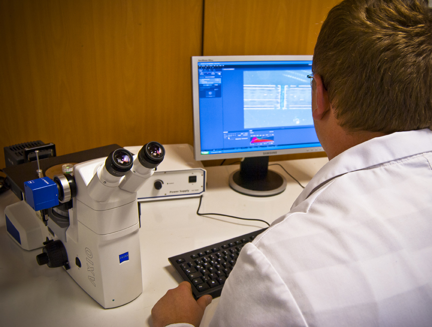
For the micro section analysis, we are using only a small part of the final PCB. For the preparation of the sample some manufacturing steps are essential. After milling, the small part is placed in a ring and poured out with epoxy resin. Subsequently, the micro section sample originates in its raw form under influence of high pressure. The next step is to make the copper visible. Under use of the grinding and polishing machine, the surface will be sanded in several work processes. After the necessary steps to create the body, the precision work takes place. For a clear and define image we are using diamond suspension for polishing and ammonia solution to bring out the copper layers more clearly.
This preparation must be done very carefully step by step, for imaging the correct area. So we can locate smallest errors under the microscope.
The micro section analysis is inclusive with the initial-sample-report. If you wish to use this as an additional service, please don’t hesitate to contact us.
 English
 German